| |
EXERCISES ON BOUNDARY-SCAN APPLET
Objectives
Three main aims are to be achieved during this laboratory work's execution. You should: 1) learn the basic elements of boundary scan architecture, 2) introduce yourself to the concepts and techniques of boundary scan and 3) perform testing and diagnosis using boundary scan.
Introduction
Widespread adoption of IEEE 1149.1 (Test Access Port and Boundary Scan Architecture) standard reflects an industry-wide need to simplify the complex problem of testing boards and systems for a range of manufacturing defects and performing other design debug tasks. In 70s and 80s the main board level test technique was the "bed of nails", which ensured the physical contact to any desired point of the circuitry. This method, however, was limited to boards with two conductive layers only. Moreover, the circuit packaging was restricted to the "dual in line". Modern PCBs (Printed Circuit Boards) have a number of inaccessible internal layers as a rule, and the modern circuit packaging includes types like various "grid arrays" (PGA - Pin Grid Array), which have a lot of inaccessible pins. These difficulties have led to introduction of the Boundary Scan standard. This standard provides a unique opportunity to simplify the design debug and test processes by enabling a simple and standard means of automatically creating and applying tests at the device, board, and system levels. There are some boundary-scan-based software tools that take advantage of the access and control provided by boundary scan architecture to ease the testing process.
The primary reasons for using boundary scan are to allow for efficient testing of board interconnect and to facilitate isolation and testing of chips either via the test bus or by built-in self-test hardware. With boundary scan, chip-level tests can be reused at the board level.
Since 1990 when the IEEE 1149.1 standard was approved, implementation of the standard has accelerated. As more people became aware of and used the standard, the need for a standard method for describing IEEE 1149.1-compatible devices was recognized. Therefore, an industry standard language called Boundary Scan Description Language (BSDL) was developed. BSDL is a subset of VHDL (Very High Speed Integrated Circuit [VHSIC] Hardware Description Language) that describes how IEEE 1149.1 is implemented in a device and how it operates. BSDL captures the essential features of any IEEE 1149.1 implementation.
Work description
The practicing will be done using the boundary scan demo applet. For the practicing you will need to choose in the applet any circuit (the several connected chips) that constitutes an interest for you. To do training you will need to execute following operations (see Steps). In this laboratory work we are going to study main principles of boundary scan testing. You will focus on the important concepts of it, such as TAP (Test Access Port) controller, the instruction and data registers and boundary scan instructions. In the last part of the work you should try to perform the interconnect diagnosis in a given board. Also, there will be given an advanced (not obligatory) task to develop a custom chip description by your own using BSDL. This task is for those students who feel an interest in it and who are good at programming on VHDL. In order to accomplish the required tasks of this laboratory work it is very useful to review the theory of boundary scan testing. Undoubtedly, it will help if you do it before starting the laboratory training. Also, after STEPS you can find an Example, which shows how one can follow them.
1. TAP controller study.
1.1 Run the boundary scan applet. After that, it automatically enters the TAP mode and the default board will be loaded too.
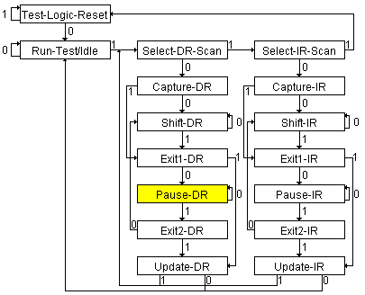
1.2 Afterwards you should try to make transitions through the state diagram of the TAP controller. The state diagram is illustrated in the right upper corner of the applet window. As you see, the starting point is the Test-Logic-Reset state. On the diagram find following states: Pause-DR and Exit2-IR, and then using TMS and TCK buttons try to go there. Continue practicing with other chosen target states.
1.3 Be sure to find the answer to the following question: what is the maximum number of clock cycles needed in order to return to the Test-Logic-Reset state from a random unknown state if you keep TMS signal constantly 1? (not mentioned in an Example)
2. The Instruction Register (IR) study.
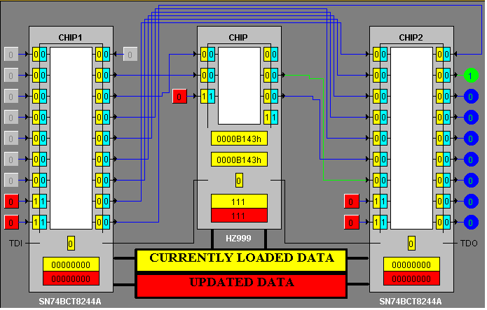
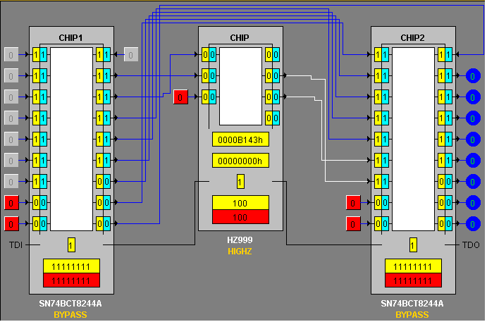
2.1 Find the IR branch on the TAP controller state diagram. Then make some necessary transitions through the state diagram in order to reach the Shift-IR state. Now, being in this state you have to load values that are defined in the step 2.2 to the IR of each chip that is currently illustrated on PCB (Printed Circuit Board) Panel. As you can see, the IR is a rectangle situated on each chip (yellow color of a rectangle shows currently loaded data, red colored rectangle means updated data).
2.2 If you have reached the Shift-IR state, load all 0's combination to the IR of the first chip using TMS and TCK signals (simply push TMS(0) and then click TCK; the number of clicks corresponds to the number of 0's you want to load to the IR). Then insert all 1's combination to the IR of the second chip (push TDI(1) and then again click TCK as much number of times as the number of 1's that you wish to be loaded to the IR) and so on. In the similar way try to fill the IRs of all chips. Note that before filling you must define sizes of all IRs. For this, just count the number of bits of all IRs. Before the last bit insertion, push TMS(1) and then using TCK make transition to the Update-IR state of the state diagram. After the transition, you can see that every IR has the same data as you have loaded into them. Thus, you have updated the contests of all IRs. Finally, you have to have all 0's combination in the IR of the first chip, all 1's combination in the IR of the second chip and so on.
3. The Data Register (DR) study.
3.1 Note that this task is only for those boards, where the ID code is defined for the one of the chips. To do the required task, please select one of these boards.
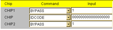
3.2 Choose Command mode under Mode menu. Afterwards, for the chip that has ID code register choose IDCODE instruction with an input 1, for other chips choose BYPASS and select any input combination you want.
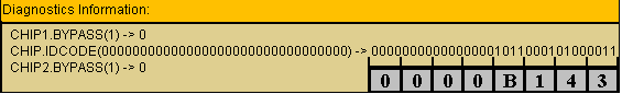
3.3 When all selections are done, push the button Scan IR and then Scan DR. After that diagnostic information should appear. Now you can see the data that you have loaded to the DR and the data that has been read on its output. As you have already noticed, the ID code represents itself a number in a hexadecimal system (for example, 0000B143h). Now you must compare this ID code with CHIP.IDCODE output value, which you must convert from a binary format to a hexadecimal system.
3.4 Answer to the following question: what does it mean if the converted value is the same as the chip's ID code? And what if it is not the same? (not mentioned in an Example)
4. Boundary Scan instructions study.
4.1 Try to understand differences between EXTEST, INTEST, BYPASS, SAMPLE, CLAMP and HIGHZ instructions. For this, review the theory and then on practice try to supplement your knowledge.
4.2 Choose EXTEST and INTEST commands for all chips. Select the test vectors. Note that you must take into account the control signals of all chips. Simulate chosen vectors: push Scan IR and then Scan DR. What information is observed on the outputs of all chips? Is there any difference between EXTEST and INTEST instructions? If yes, name it? Which of these instructions is optional, and which is mandatory? (not answered in an Example)
4.3 Perform similar tests with other instructions. Try to analyze the diagnostic information after their simulation. Find out what purposes these instructions are used for. How do you think why some of them are mandatory and some are optional instructions?
5. The interconnect diagnosis.
5.1 Choose Command mode under Mode menu. Afterwards, choose Mode à Random fault under Diagnostics menu. By this, you have inserted a random fault on one of the wires.
5.2 In order to perform the interconnect diagnosis we must set up all the chips in EXTEST mode. Now we need to select the proper test vectors taking into account the control signals of all chips. Selection of the right values of the control signals guarantees us that all outputs of the chips will not change to a high-impedance state.
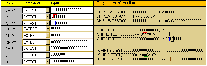
5.3 Okay, let's select the inputs for all chips. Let the first input pattern for all chips consist of all 1's. After the selection, push Scan IR and then Scan DR. Now the simulation process has started and after a few moments the diagnostic information should appear. But that is not all. Now select the second pattern for all chips. Let it consist of all 0's. After you have selected it, push Scan IR and then Scan DR like it was done in case of the first simulation. After the second simulation, repeat the second step with all 0's patterns again. In the end, we should get the proper diagnostic information for the 3 simulation processes.
5.4 Analyze the diagnostic information for the last 2 simulations. Try to answer to the following question: why the results of only the last 2 simulations should be analyzed? Find the random error you have inserted and then click on the proper connection wire (you should see the name of this wire). Afterwards, choose Give the answer under Diagnostics menu, and select the name of the wire with the same name. The applet tells you if your answer is correct or not.
6. Chip development using BSDL (advanced).
6.1 Choose Edit chip à Custom under Edit menu. Insert the name for a new chip. Now you can enter the BSDL description. The SSBDD (Structurally Synthesized Binary Decision Diagram) model is not necessarily to be inserted. The latter format is optional since for the simulation of the most boundary scan modes the internal structure of the chip can be neglected.
6.2 When the step 6.1 is done, the following actions are likely to be executed: a verification of a new chip and then its simulation.
Here we will follow the Steps of the present laboratory work. The last (advanced) step will not be shown. In this example we will practice with a default board, which has 3 chips on it.

1. TAP controller
study.
1.1 When the applet has been loaded, we set to the step 1.2.
1.2 According to the required task, it is necessary to go to the following states on the diagram: Pause-DR and Exit2-IR. For this, we use TMS and TCK buttons. Suppose, we have chosen Pause-DR for our target state. At first, we must find the states on the diagram through which we could reach this state. Thus, these states are: Run-Test/Idle, Select-DR-Scan, Capture-DR, Shift-DR, and Exit1-DR. In order to be in Run-Test/Idle state we need TMS(0) to be chosen and then we push TCK button. After the transition the next state to reach is Select-DR-Scan. As you see on the diagram, we need to choose TMS(1). After that, we push TCK button in order to make a transition. Now we are in Select-DR-Scan state. Further try to make the rest of necessary transitions to reach Pause-DR state and then return back to Test-Logic-Reset state. Use the logic that is described above. See the figure below, which illustrates our target state's Pause-DR location on the diagram.
2. The Instruction Register (IR) study.
2.1 Suppose, we are in Shift-IR state on the diagram. Now we need to load some values that are defined in the step 2.2 to the IR of the each chip on the board. Thus, we set to the next step.
2.2 So, let us define the number of bits for all IRs: for CHIP1 and CHIP2 the sizes are equal to 8 bits and CHIP has a 3-bit IR. Thus, we need to load to the registers of CHIP1 and CHIP2 eight 0's, and to CHIP register the test pattern of three 1's. Moreover, we have to remember that the direction of data flow through the chips is from left to right. It means that the first IR to fill is a CHIP2 register, then CHIP IR, and the last is CHIP1 register. Suppose, we have entered the test patterns for all IRs. If you have done all the actions (the rules for a vector insertion are mentioned in a task step) correctly, you must get the same figure as you can see below.
3. The Data Register (DR) study.
3.1 As the default board has been loaded, we see that the ID code is defined only for CHIP (the ID code is illustrated in the center of it).
3.2 Now we need to select the inputs for all chips. For this, see the figure below.
3.3 Afterwards, we push the button Scan IR and then Scan DR. After the simulation, we have got the diagnostic information (see the figure below together with analyze information). After its analysis, we have convinced that the converted value of CHIP output is the same as the chip's ID code (0000B143h).
4. Boundary Scan instructions study.
4.1 Suppose, we have reviewed the theory about following instructions: EXTEST, INTEST, BYPASS, SAMPLE, CLAMP and HIGHZ.
4.2 This task is to be executed by your own. Please, see the step 4.3.
4.3 Let's choose HIGHZ and BYPASS instructions and study them. The theory says that HIGHZ instruction is used, for instance, when an in-circuit test is required for testing a non-BS compliant component; BYPASS instruction is also very useful, because it permits bypassing of the current circuit and places the one-bit bypass register between TDI and TDO of the chip when another circuit is being tested. Now, let's practice with these instructions. Suppose, we have done some necessary selections that are illustrated in the figure below. On PCB Panel (the second figure below), we can see that all CHIP wires are in a high-impedance state indeed (these wires are white colored). Thus, we have studied HIGHZ and BYPASS instructions on practice.
5. The interconnect diagnosis.
5.1 Let us insert a random fault into the circuit.
5.2 Next we set up all the chips in EXTEST mode and select the proper test vectors. The control signals of all chips must be 0 valued.
5.3 As it is written in the task, we should get the proper diagnostic information for the 3 simulation processes. Suppose, we have done this and got some results. For this, see the figure below, which illustrates chosen inputs and the corresponding diagnostic information.
5.4 Let's analyze the diagnostic information for the last 2 simulations. We must compare the diagnostics information (namely the chips output values) of the second simulation with the input values of the previous step. The same manipulation is also applied for the third received diagnostics information, which we should compare with the input values of the second simulation. Okey, we start with CHIP.EXTEST output (2 bits that are framed by red rectangle). As you see, there is a 0 valued bit before these 2 bits. It is a control bit, so we do not pay our attention on it. Now take a look at the input pattern of the first simulation. It is clear that 2 bits in an input pattern of the first simulation are the same that were read on CHIP.EXTEST output. It means that there is no error occurred. Now we set to CHIP2.EXTEST output (8 bits that are framed by blue rectangle). Again, as it was done earlier, we do not pay attention on first 2 control bits. Instead, we look at the corresponding input pattern of the previous simulation. We have entered eight 1's, but when comparing it with CHIP2.EXTEST output, we realize that this chip's output is not the same as an input pattern. The difference is in the second bit: we have entered 1 value for this bit, but on output 0 valued bit has occurred. Thus, we have discovered the randomly inserted fault and it is stuck-at 0. Afterwards, by clicking on the corresponding wire, we find the name for it, which is S2B. The applet has confirmed our proposition: the fault has occurred on the connection wire S2B indeed. Now there is no need to analyze the rest of the diagnostics information.
| |
|
|
Last update: 3 August, 2004